
Faulty mobile phones and solar cells could soon be a thing of the past thanks to a ground-breaking invention developed at The Australian National University (ANU).
Engineers have developed a powerful new tool to help manufacturers spot defects or unwanted features in everyday technology – such as mobile phones, batteries and solar cells – more easily and much earlier in the fabrication process.
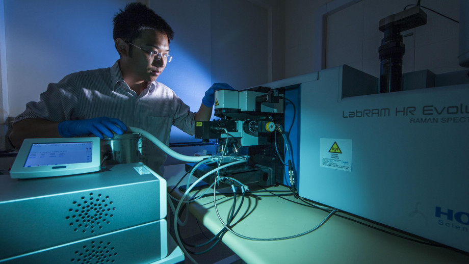
According to lead author Dr. Hieu Nguyen, the invention works by capturing high-resolution images of semiconductor materials, including many potential defects, within seconds.
“We’re calling it ‘the miracle of speed and space’. It’s not just several times faster than techniques currently being used – it’s tens of thousands of times faster,” said Nguyen, from ANU Research School of Electrical, Energy and Materials Engineering.
“This opens the door to a new generation of ultra-high resolution, precise characterisation and defect-detection tools for both research and industry sectors.”
The ANU researchers, in collaboration with scientists from the National Renewable Energy Laboratory in the U.S., discovered the light emitted from various semiconductor materials, including silicon, perovskites
Once this light is captured on camera, the optical images can be used to gather important information about how the material works.
“Now we know much more about the property of the light – and, just from the image, we can extract different information with incredible depth,” he said.
“The beautiful part of this research is that we used ordinary tools that are commercially available, and converted them into something extraordinary.”
The team demonstrated the method by capturing images of the optical bandgap, one of the first pieces of information researchers need to know about a material.
This bandgap determines many properties of semiconductors, including the ability to absorb light and conduct electricity.
“We tested this invention extensively on various state-of-the-art perovskite solar cells made here at ANU and independently confirmed the results with many other low-speed or low-resolution techniques. They matched perfectly,” he said.
“We are refining the invention so that it can be commercialized.”
“Before this invention, it took an entire week to get a high-quality bandgap image on a device. Now, with our invention, it takes just a few seconds to get an image with the same quality,” said co-author Boyi Chen from ANU.
“This invention will help to produce more robust mobile phones, solar cells, sensors and other optical devices as it can spot defects very early in the fabrication process.”
The research paper has been published in Advanced Energy Materials and is available online.